


Why GW-Scale PV Manufacturing Demands Standardized Laser Equipment
For gigawatt scale photovoltaic production lines, having standardized laser equipment isn't just preferred but absolutely necessary because of several key manufacturing reasons. First off, when all the equipment matches up, it makes everything work together smoothly without those annoying compatibility issues that can actually cut yields by around 15 to 20 percent according to recent studies from NREL on thin film production in 2023. Then there's maintenance stuff too. Plants using standard parts see technicians fixing problems about 30% quicker since they don't have to deal with different kinds of laser modules or control panels every time. And let's not forget about scaling up operations. Big GW scale lines need lasers that perform predictably day after day. These massive operations run nonstop and require laser systems that consume pretty much the same amount of energy each time (within about plus or minus 5%) otherwise companies face serious grid instability fines that can top $740,000 per year as reported by Ponemon Institute in their 2023 risk assessment report. This whole approach to laser equipment for PV manufacturing helps tackle those pesky throughput problems that plague many factories.
- Unified data protocols enabling real-time process synchronization
- Interchangeable optical components reducing spare part inventories by 40%
- Repeatable beam quality parameters ensuring <0.2% cell efficiency deviation
Without standardization, GW-scale lines face exponential risk escalation—each unique equipment variant increases process anomaly rates by 11% (NREL, 2024 PV Manufacturing Systems Benchmarking Study). This foundational approach directly enables the 12-unit PV GW-Scale Laser Equipment Standard, transforming production line planning from custom engineering projects into replicable industrial solutions.
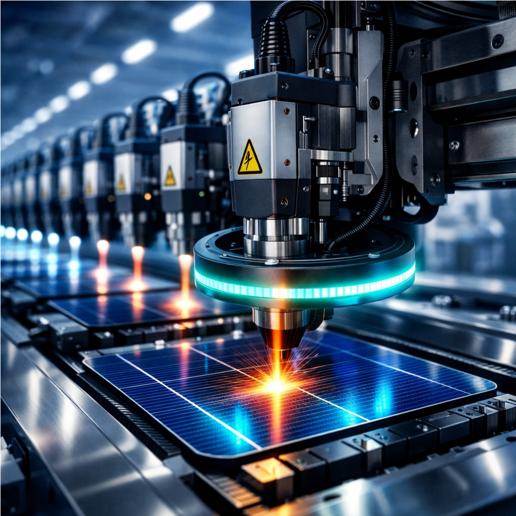
The 12-Unit PV GW-Scale Laser Equipment Standard: Core Functions & Integration Logic
This standardized configuration integrates 12 specialized laser modules with co-located inspection systems to optimize photovoltaic manufacturing at gigawatt scale. Each unit pairs a critical laser process with immediate quality verification—eliminating standalone inspection stations while sustaining throughput exceeding 1.2 GW annually (NREL, 2023 Thin-Film Production Benchmarks).
Laser Texturing + Real-Time Surface Inspection
Integrated optical coherence tomography scans surfaces during texturing, detecting deviations from optimal pyramid patterns in real time. Closed-loop adjustment maintains consistent light-trapping efficiency and reduces material waste by 9% compared to post-process inspection.
Laser Edge Isolation + Microcrack Detection Module
High-speed thermal imaging identifies microcracks during edge isolation as laser scribes non-conductive boundaries. The system automatically flags cells with subsurface fractures exceeding 5 μm—preventing hot-spot failures—while maintaining 0.4-second cycle times per wafer.
Laser Contact Opening (LCO) + Pattern Fidelity Verification
Machine vision verifies contact opening geometry within ±2 μm tolerance during LCO processing. Real-time pattern analysis ensures precise emitter alignment, boosting cell efficiency by 0.3% absolute and preventing metallization defects responsible for 17% of yield losses (PV Manufacturing Insights, 2024).
The configuration’s synchronized data flow enables continuous process refinement across all stages, with integrated sensors feeding performance analytics to central control systems. This architecture reduces manual intervention by 65% while maintaining 99.4% uptime in GW-scale production environments.
Inspection-Centric Integration: Ensuring Traceability from PL to Final Classification
GW-scale PV manufacturing requires seamless data integration between laser processing and quality inspection stages. This closed-loop approach enables real-time defect tracking—from photoluminescence (PL) imaging through final cell classification—preventing error propagation across production batches.
Photoluminescence-Guided Laser Process Correction Loops
Photoluminescence imaging can spot those hidden flaws beneath the surface that regular eyes just cant catch microcracks and bunches of impurities lurking where they shouldn't be. Hook it up to laser systems and suddenly we get these automatic tweaks happening in real time. The system will dial back the power when dealing with thinner wafers or crank up the scanning speed around those tricky edge areas. These smart adjustments have been shown to slash defects caused during processing by about 19 percent without slowing things down too much according to some recent research from NREL on thin film yield improvements back in 2023.
Multi-Modal Defect Mapping Across Laser Processing Stages
When manufacturers combine photoluminescence testing with electroluminescence and thermal imaging techniques, they get these unique defect profiles for every solar cell. The process maps out issues in laser texturing right back to problems with contacts later on in production, which helps figure out what's actually causing defects. Most plants report around 99.7% traceability when tracking cells from their first PL scan all the way through to final sorting. This matters a lot for big scale operations running gigawatt level laser systems because even a small 0.1% drop in yield can mean losing about one megawatt of production each day. That kind of impact makes these advanced inspection methods absolutely essential for modern manufacturing lines.
Data-Driven Optimization: CPV and Real-Time Analytics in PV GW-Scale Laser Lines
When real time analytics get applied to those massive PV GW scale laser lines, it turns what used to be just static manufacturing processes into systems that can actually optimize themselves on their own. These systems tackle something called Cell-to-Process Variation or CPV head on. What happens is continuous streams of sensor data track everything from laser settings to how materials react and even environmental conditions. All this information gets fed into machine learning algorithms that spot problems early and make corrections before anything affects production yields. Take for instance when we look at the plasma emissions during laser contact opening operations. By analyzing these spectra, the system automatically tweaks pulse energy levels so the silicon gets ablated at just the right depth. This approach has been shown to cut down microcracks by about 18 percent according to research published by NREL in their 2023 field validation study on adaptive laser processing techniques.
This closed-loop intelligence enables two critical advancements:
- Predictive Process Calibration: Algorithms correlate laser texturing patterns with subsequent metallization adhesion failures, automatically refining beam profiles to prevent downstream defects.
- Energy-Performance Balancing: AI models optimize power consumption against throughput targets, cutting energy waste by 22% while maintaining 0.5% efficiency gains across production batches.
Research supported by the Department of Energy showed that when they analyze laser lines across 12 units using spatiotemporal methods, it cuts down on performance losses about 1.2 percent each year because they can fix drift issues as they happen (DOE Solar Energy Technologies Office, Advanced Manufacturing R&D Portfolio, 2020). Another study found similar results where companies used big data predictions for maintenance schedules. These smart approaches cut wasted materials by around 15% in test runs at gigawatt scale production lines according to Sustainability journal volume 10 issue 4 from 2018. What these findings really mean is that standardizing equipment isn't just about making sure all parts are the same anymore. Instead, manufacturers now need systems that can handle unexpected problems while still maintaining quality standards throughout their operations.
Frequently Asked Questions (FAQ)
Why is standardized laser equipment crucial for GW-scale PV manufacturing?
Standardized laser equipment is essential because it minimizes compatibility issues, reduces maintenance time, ensures predictable performance, and tackles throughput problems effectively.
What is the 12-Unit PV GW-Scale Laser Equipment Standard?
This standard consists of 12 specialized laser modules integrated with inspection systems to optimize manufacturing at gigawatt scale, focusing on real-time verification and maintaining high throughput.
How do real-time analytics impact PV GW-scale laser lines?
Real-time analytics transform static processes into self-optimizing systems, tackling Cell-to-Process Variation and improving yield through predictive process calibration and energy-performance balancing.
Table of Contents
- Why GW-Scale PV Manufacturing Demands Standardized Laser Equipment
- The 12-Unit PV GW-Scale Laser Equipment Standard: Core Functions & Integration Logic
- Inspection-Centric Integration: Ensuring Traceability from PL to Final Classification
- Data-Driven Optimization: CPV and Real-Time Analytics in PV GW-Scale Laser Lines
- Frequently Asked Questions (FAQ)