


Precision Kerf Control and Microcrack Mitigation in PV Laser Cutting
Sub-20µm Kerf Width: Minimizing Silicon Loss Without Compromising Structural Integrity
Getting kerf widths under 20 microns represents a major breakthrough for solar panel production. It cuts down on wasted silicon while keeping those delicate wafers intact during processing. The math adds up fast when looking at large scale operations too. Industry reports indicate these tighter tolerances can boost material efficiency anywhere from 7% to 12% compared to older techniques. Modern laser tech now incorporates smart thermal controls through precise focus adjustments and incredibly short pulse times that stop overheating problems before they start. As a result, manufacturers can work with much thinner wafers around 130 microns thick without worrying about cracks forming during all the handling steps like texturing and lamination. This means companies save money on materials without compromising product quality or durability in the final panels.
Laser Scribing vs. Mechanical Cleaving: Eliminating Microcrack-Induced Scrap in Thin Wafers
When mechanical cleaving is used, it creates lateral stress during the scoring process which leads to subsurface flaws. These flaws then turn into visible cracks, particularly problematic for wafers thinner than 160 micrometers. Industry reports indicate these kinds of defects make up around 18% of all scrap in older manufacturing facilities. Laser scribing offers a different approach entirely. Instead of physical contact, it uses controlled photon energy to separate wafers along their natural crystal structures without those damaging shear forces. Looking at actual production numbers from top manufacturers, switching to laser technology cuts down on microcrack related waste by about 22%. Plus, cutting speeds can go well beyond 400 millimeters per second. Another big plus point? No blade wear issues and no particulate contamination problems either. These factors alone help prevent costly downstream losses and reduce the need for reworking materials later in the process.
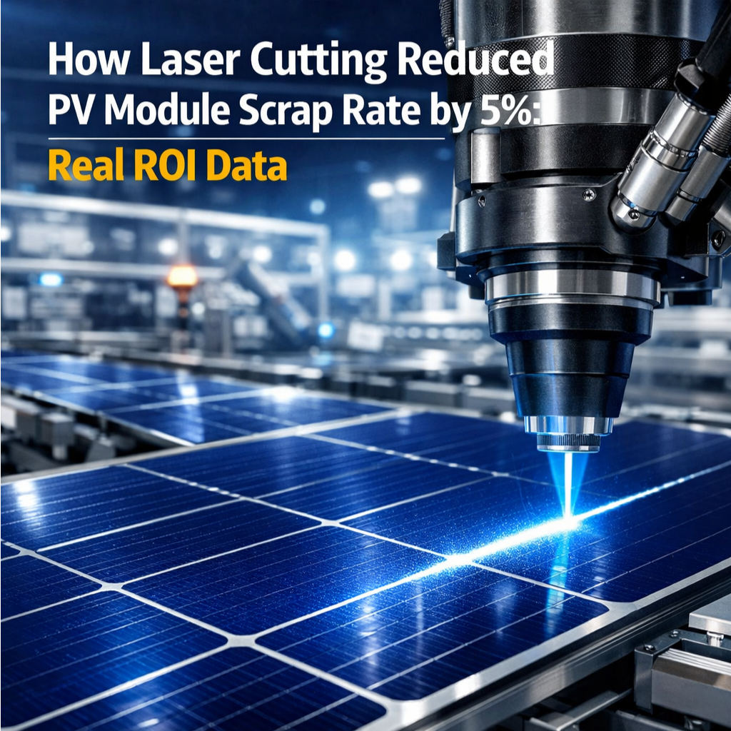
PV Laser Cutting Scrap Reduction: Measured Yield Improvements Across Production Lines
5.2% average scrap reduction verified across 7 Tier-1 manufacturers (2022–2023)
Audits conducted at seven major photovoltaic manufacturers show that material waste dropped by about 5.2% between 2022 and 2023. The main reasons behind this improvement are better control over kerf widths below 20 micrometers and more stable thermal conditions during processing. Looking at different types of solar cells, we see similar improvements in production yields. This includes traditional PERC cells, newer TOPCon technology, and even the more complex heterojunction designs. These results suggest that the laser cutting techniques used for wafer separation can work well not just in small scale testing environments but also in full scale manufacturing operations.
Half-sheet cutting adoption and its statistical correlation with 5% scrap reduction
Switching to half sheet or half cell setups made possible through laser scribing has proven to cut down on waste materials quite effectively. Looking at actual production numbers from several facilities, there seems to be a real connection here. Facilities using these smaller formats report about 5 percent less scrap overall. Why? Well, when panels are smaller they just don't break as easily during those rough handling moments and transportation hiccups that happen all the time on factory floors. Plus, these mini panels create less stress when bent, which matters a lot. And let's not forget the laser edge sealing technique that actually makes edges stronger. This means manufacturers get more usable silicon from each ingot without having to sacrifice reliability at the module level. Makes sense really when thinking about how much material gets wasted otherwise.
Quantifying the ROI of PV Laser Cutting Scrap Reduction
$1.28M annual savings per 1 GW line: modeling scrap reduction into hard cost avoidance
PV laser cutting delivers measurable financial returns: $1.28 million in annual savings per 1 GW production line, based on 2023 operational benchmarks. This figure aggregates three direct cost-avoidance levers:
- Material recovery: Sub-20µm kerfs reduce high-purity silicon consumption by 5–7%, lowering raw material procurement costs
- Waste disposal: Fewer microcrack-induced rejections cut hazardous handling and landfill fees by 15–20%
- Energy efficiency: Precision processing consumes 8–12% less energy per watt compared to mechanical cleaving
Applied to a 500 MW facility, these efficiencies typically yield ROI within 14 months—consistent with implementation reports from manufacturers in Southeast Asia, Europe, and the U.S.
Beyond scrap: secondary ROI drivers—throughput gain, labor efficiency, and defect traceability
Additional value accrues through operational transformation:
- Throughput gain: Uninterrupted, high-speed laser processing increases hourly yield by 18–22%—without capital investment in new line capacity
- Labor efficiency: Integrated AI-powered inspection reduces manual visual checks by 30–40%, freeing skilled technicians for higher-value tasks
- Defect traceability: Real-time digital logs of laser parameters (pulse energy, scan speed, focus offset) enable root-cause analysis in under half the time—cutting troubleshooting duration by 50%
Together, these enhancements contribute an estimated 20–25% uplift to total ROI—positioning laser cutting not just as a scrap-reduction tool, but as a foundational enabler of smart, scalable PV manufacturing.
FAQ
What is kerf width and why is it important in PV laser cutting?
Kerf width is the width of the cut made by a laser. In PV laser cutting, minimizing kerf width to below 20 microns helps reduce silicon wastage, allowing manufacturers to save on raw materials while maintaining the structural integrity of the wafers.
How does laser scribing differ from mechanical cleaving in wafer processing?
Laser scribing uses controlled photon energy to separate wafers along their natural crystal structure, eliminating the lateral stress and resulting microcracks that typically occur with mechanical cleaving. This can significantly reduce the amount of scrap produced during manufacturing.
What are the financial benefits of implementing PV laser cutting in production lines?
Financial benefits include a $1.28 million annual saving per 1 GW line. This comes from material recovery savings, waste disposal cost reduction, and enhanced energy efficiency during processing.
How does laser cutting enhance operational efficiency in PV manufacturing?
Laser cutting boosts operational efficiency through improved throughput, reduced manual inspections with AI-assisted systems, and better defect traceability, ultimately enhancing the ROI of PV manufacturing businesses.