


How advanced laser scribing enables solar cell manufacturers to transition from PERC to TOPCon technology, achieving over 25% efficiency with precise dielectric opening and selective emitter doping. Learn about wavelength selection, pulse control, and real production results.
The Efficiency Imperative Driving Laser Innovation
The photovoltaic industry is racing toward higher conversion efficiencies. Every 0.1% gain in cell efficiency translates into millions of dollars in revenue for large-scale manufacturers—and a competitive edge in a market driven by levelized cost of electricity. This relentless pursuit has pushed cell architectures from the long-dominant PERC (Passivated Emitter Rear Cell) to the emerging TOPCon (Tunnel Oxide Passivated Contact) and beyond.
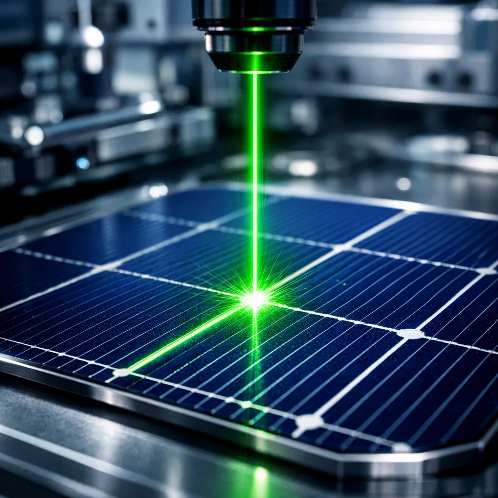
At the heart of this transition lies a manufacturing process often overlooked but critically important: laser scribing. Whether opening dielectric layers on PERC rear sides or doping selective emitters for TOPCon, the laser's precision directly determines final cell performance. A line width variation of just 10μm can shift efficiency by 0.15%. A poorly controlled heat affected zone can create recombination centers that degrade voltage. As cells become more efficient, they also become more sensitive to laser damage.
For production managers and process engineers, the challenge is clear: the laser equipment that delivered 22.5% PERC cells may not be adequate for 25%+ TOPCon targets. Understanding how laser parameters—wavelength, pulse duration, beam profile—interact with evolving cell architectures is essential for making smart capital investments and avoiding costly performance bottlenecks.
How Laser Requirements Evolve from PERC to TOPCon
PERC: Rear-Side Passivation Opening
PERC cells, which still represent over 80% of global production capacity, rely on laser scribing for one primary task: opening the rear dielectric stack (typically Al₂O₃ and SiNₓ) to allow aluminum to form the back surface field. The laser selectively removes these layers without damaging the underlying silicon.
For this application, the requirements are well established:
- Line width: 40–60μm openings, balancing contact area against passivation integrity
- Wavelength: 532nm green is preferred for its strong absorption in dielectrics and moderate penetration in silicon
- Pulse duration: Nanosecond (typically 10–100ns) provides sufficient energy for clean ablation
- Opening area: 15–25% of the rear surface, optimized for contact resistance versus surface recombination
The process window is forgiving enough that many PERC lines still operate with 1064nm IR lasers, though green systems generally offer cleaner edges and slightly higher efficiencies.
TOPCon: Adding Selective Emitter Doping
TOPCon cells introduce a fundamentally different laser requirement: selective emitter formation. Beneath the front contacts, the cell needs heavily doped regions (p+) to reduce contact resistance and minimize carrier recombination. These regions are created by laser doping—simultaneously opening the dielectric and driving dopants into the silicon.
This adds several layers of complexity:
- Doping control: Target sheet resistance of 80–120Ω/, junction depth 0.3–0.5μm
- Line width evolution: Narrower lines (60–100μm) to minimize recombination area
- Damage minimization: Crystal damage from laser pulses must be avoided to maintain bulk lifetime
- Uniformity: Doping concentration must be consistent across the entire wafer to avoid cell mismatch
Where PERC lasers could tolerate some silicon damage as long as the dielectric was removed, TOPCon demands a gentler touch. The laser must deliver enough energy to drive dopants but not so much that it creates defects. This has driven adoption of MOPA (Master Oscillator Power Amplifier) fiber lasers with pulse-width adjustability from 2–500ns, allowing fine-tuning of thermal input.
HJT and Future Requirements
Looking ahead, heterojunction (HJT) and back-contact (IBC) cells will push laser requirements even further. HJT uses temperature-sensitive amorphous silicon layers that cannot tolerate nanosecond thermal processing. This is driving interest in picosecond and femtosecond UV lasers that remove material via cold ablation with virtually no heat affected zone—essential for maintaining passivation quality while creating contact openings.
Matching Laser Parameters to Cell Architectures
Wavelength Selection
Green (532nm) remains the dominant choice for both PERC and TOPCon scribing. Its absorption depth in silicon (~1μm) is shallow enough to confine energy to the surface region, yet deep enough to enable controlled doping. Commercial 532nm lasers with 30–50W power are mature, reliable, and capable of >8,000 cells per hour throughput.
Infrared (1064nm) has deeper penetration (hundreds of microns) and is generally avoided for front-side processing due to risk of bulk damage. However, some manufacturers use IR for specific doping applications where deeper junctions are desired, or for rear-side processes where silicon damage is less critical.
Ultraviolet (355nm) is increasingly used for advanced applications. Its absorption depth is <100nm, confining energy to the surface and enabling extremely fine features. UV is essential for HJT and for processing ultra-thin wafers (<120μm) where nanosecond pulses could cause breakage.
Pulse Duration and MOPA Flexibility
The shift from PERC to TOPCon has elevated the importance of pulse control:
- Fixed nanosecond lasers (50–100ns) are simple and robust but offer limited tuning. They work well for PERC ablation but may create excessive thermal stress for TOPCon doping.
- MOPA fiber lasers allow independent adjustment of pulse duration (typically 2–500ns) and frequency. This enables process optimization: shorter pulses for cold ablation of dielectrics, longer pulses for thermal diffusion during doping. One TOPCon manufacturer using a MOPA source reported 0.3% absolute efficiency gain compared to a fixed-pulse laser on identical cell designs.
Picosecond lasers (<100ps) operate in the cold ablation regime. Heat diffusion is negligible, eliminating micro-cracks and edge recombination. Though currently slower and more expensive, they are essential for HJT and are gradually being adopted for TOPCon R&D lines.
Beam Shaping for Uniformity
Gaussian beams, with their hot center and cool edges, create non-uniform line profiles—the center may over-ablate while edges leave residual dielectric. This non-uniformity directly impacts doping consistency and contact formation.
Flat-top beam shaping, achieved through diffractive optical elements (DOEs), transforms the beam into a uniform intensity profile. The result is consistent line depth and doping across the entire scribe width. Production data shows flat-top beams reducing efficiency variation across a cell from ±0.2% to ±0.05%, a critical advantage for large-scale manufacturing where every wafer must perform identically.
Real-World Applications in PERC and TOPCon Production
Case Study: PERC Line Optimization
A Chinese solar manufacturer operating a 2GW PERC line was seeing efficiency drift between shifts due to inconsistent laser opening. Their existing IR nanosecond lasers produced line widths varying from 45μm to 65μm, causing contact resistance fluctuations.
By upgrading to 532nm MOPA lasers with flat-top beam shaping (PowerScribe-P series), they achieved line width control of 50μm ±3μm across all wafers. The more uniform openings improved aluminum back surface field formation, boosting average cell efficiency from 23.2% to 23.4%—a 0.2% gain worth approximately $2 million annually for the 2GW line. The upgrade paid for itself in under six months.
Case Study: TOPCon Pilot Line Implementation
A European research center transitioning from PERC to TOPCon needed a laser system capable of both dielectric opening and selective emitter doping. They selected a 30W MOPA green laser (PowerScribe-T) with pulse control from 4ns to 200ns and integrated DOE beam shaper.
During development, they optimized two-step process:
A short pulse (8ns) at high intensity to open the SiNₓ layer with minimal silicon interaction
A longer pulse (80ns) at lower intensity to drive boron dopants from the spin-on source into the exposed silicon
The resulting selective emitters achieved sheet resistance of 95Ω/ ±5Ω/ across the wafer, with junction depth of 0.4μm. Cell efficiency reached 25.1% on 182mm wafers—matching the best results from dedicated diffusion furnaces but with significantly simpler processing.
The system's built-in process monitoring tracked pulse energy and beam position in real time, ensuring repeatability across thousands of wafers. IQ/OQ validation documentation provided by the equipment supplier (GuangYao Laser) accelerated the research center's technology transfer to production partners.
Case Study: High-Volume TOPCon Production
A TOPCon manufacturer in Southeast Asia ramping to 5GW capacity needed laser scribing tools that could maintain 25.0%+ efficiency at production scale. They installed 16 dual-stage laser systems (PowerScribe-T) capable of 8,500 cells per hour each, with automated wafer handling for 130μm thin wafers.
Key performance metrics after six months of production:
- Average cell efficiency: 25.15%
- Efficiency variation across production: ±0.08%
- Breakage rate: 0.018% (significantly below the 0.03% industry benchmark)
- Uptime: 97.5% including scheduled maintenance
The manufacturer attributed the low breakage rate to the system's non-contact air-bearing transport and real-time crack detection, which rejects damaged wafers before laser processing. The high uptime was supported by remote diagnostics and a local service team with stocked spare parts—part of PrecisionLase's global support network.
Key Advantages of Advanced Laser Scribing Systems
Precision and Consistency
Modern laser scribing tools deliver line width control within ±5μm and alignment accuracy of ±15μm across full wafers. Flat-top beam profiles ensure uniform doping and ablation, eliminating the hot spots and cold edges that cause performance variation. Real-time power monitoring maintains energy stability within ±2% over multi-shift runs.
Production Efficiency
Dual-stage processing—marking one wafer while handling the next—enables throughput >8,500 cells per hour without compromising accuracy. Scan speeds reach 50 m/s with galvanometer control, and automated recipe changeovers allow different cell types to run back-to-back with minimal interruption.
Material Flexibility
As wafer thickness drops below 130μm for TOPCon and 100μm for HJT, mechanical stress becomes critical. Laser systems with optimized acceleration profiles and non-contact handling achieve breakage rates below 0.02%—essential for profitable thin-wafer production. The ability to adjust pulse parameters also allows processing of different silicon substrates (mono, multi, cast) without hardware changes.
Future-Ready Design
The fastest-moving manufacturers are investing in laser platforms that can adapt to next-generation cells. Upgrade paths include:
- MOPA pulse control for evolving doping requirements
- UV or picosecond laser integration for HJT
- AI-driven process control that learns from inline metrology and automatically adjusts parameters to maintain target efficiency
PrecisionLase: Your Partner in Solar Cell Laser Processing
Behind every high-efficiency solar cell is a laser process that has been meticulously engineered. PrecisionLase, powered by GuangYao Laser's decade of industrial laser experience, brings that engineering depth to photovoltaic manufacturers worldwide.
Since 2015, GuangYao Laser has invested 15% of annual revenue into core laser source and application research—including dedicated photovoltaic process development. Our 15,000 m² Shenzhen R&D and manufacturing campus houses over 200 employees, with 50 engineers focused on laser-material interactions for solar applications. This investment has resulted in laser scribing systems that now process millions of solar cells daily across Asia, Europe, and North America.
Our photovoltaic laser portfolio includes:
- PowerScribe-P series: Optimized for PERC rear-side ablation, with 532nm nanosecond lasers and throughput >8,500 UPH
- PowerScribe-T series: Designed for TOPCon selective emitter formation, featuring MOPA pulse control (2–500ns) and integrated DOE beam shaping
- PowerScribe-U series: Ultrafast (picosecond) UV lasers for HJT and advanced cell development
Every system ships with comprehensive process documentation and IQ/OQ validation protocols, helping customers accelerate ramp-up and maintain quality control. Our global service network—with hubs in Shenzhen, the USA, and Germany—provides 24/7 technical support, remote diagnostics, and on-site service within 48 hours for most locations.
Conclusion: Choosing the Right Laser for Your Technology Roadmap
The transition from PERC to TOPCon is not a single event but a journey. Each step brings new demands on laser precision—from dielectric opening to selective doping to ultra-fine patterning. The equipment choices made today will either enable or constrain future efficiency gains.
For manufacturers focused on PERC production today but planning TOPCon migration within 24 months, the smart investment is a laser platform with MOPA capability and upgrade paths. For those already in TOPCon volume production, systems with flat-top beam shaping and real-time process monitoring deliver the consistency needed for 25%+ yields. And for R&D teams exploring HJT or back-contact architectures, picosecond UV lasers provide the cold processing essential for tomorrow's cells.
Whichever path your roadmap follows, the right laser partner brings not only hardware but also process expertise, validation support, and a commitment to continuous improvement. PrecisionLase offers exactly that partnership—proven across hundreds of photovoltaic lines worldwide.
Ready to optimize your solar cell laser scribing? Contact PrecisionLase for free line analysis, sample processing on your wafers, and consultation with engineers who have optimized over 100 PV production lines globally.